
Advanced Technology Funktionen (Kostenoption)
Unterstützt Starr-Flex, Chip on Board und Embedded Components
Kostenlose Demoversion
Überzeugen Sie sich von der einfachen, übersichtlichen und intuitiven Bedienung der PULSONIX EDA Software.
Bestellen Sie noch heute die kostenlose Demolizenz.
Präsentation der Pulsonix Funktionen
Wir bieten regelmässig online Webinare an, in denen wir die Software vorstellen.
Lassen auch Sie sich von diesem hervorragenden und kostengünstigen Produkt ünerzeugen und melden Sie sich an.
Donnerstag 15 Uhr und Freitags 11 Uhr
Senden Sie Ihre Anmeldung an:
oder rufen Sie uns an:
+49 241 56 30 23
|
|
|
Starr-Flex Technologie
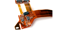
True Flexi-rigid support is available using the features within the Advanced Technology package; Multi-spanned Layer Areas, Board Outlines, Board Cutouts and Layer Spanned Components. Using these powerful options, Board outlines can be created to span 'internal' flexi layers that are still exposed externally.
Layer Spanned Components
Adding Components to layer spans allow them to also be exposed. Components on inner flexi layers can be achieved but with true 'side' and layer characteristics available within their Properties. This means accurate assembly reports, manufacturing plots and precise build details can be exported for accurate manufacturing.
Erweiterter Lagenaufbau
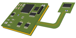
Advanced layer span definitions enable you to create the regular board outline plus the board outline required for an inner flexi-layer which may extend outside of the normal board boundaries.
Chip-On-Board Technologie
Erweiterter Regeln
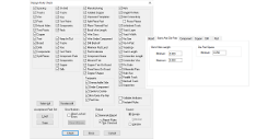
Pulsonix contains a set of rules that are obeyed using both the Online DRC and batch DRC processes. Rules can be set for min and max length of the bond pad from the die pad, and for the crossing over of bond wires. Conditional Spacing rules can be defined for COB devices that use smaller values for this type of detailing. This is also a highly desirable requirement where mixed conventional and bare die technologies are used.
Chip-On-Board
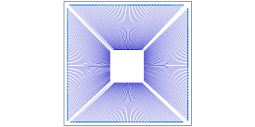
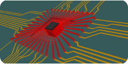
The Chip-On-Board option provides features for creation and annotation of die & bond pads and bond wires. It also allows automatic placing bond pads around the die. Within the Pulsonix design the bond pads are treated as special pads and can move independently of die and normal pads.
Bauteil Interaktion
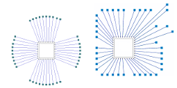
Components which contain die and bond pads are handled intelligently using an advanced rule set. Bond pads can be interactively moved independently of the main die 'body'. This movement is controlled using the min and max length rules of the bond wire, with cross-over rules also maintained in this process. The chip die can also be moved independently of the bond pads and position reset if needed.
Micro-Via Entry Pads
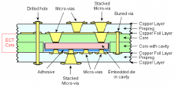
Pad styles for Micro-via use can be created using the normal pad styles dialog. However, from within this, special pad styles can be specified for Micro-via Entry Pads and Micro-via Stop Pads on different layers where the landing layer for the laser drill is to be a solid pad. The technique enables stacked Micro-vias to be created where multi-drilling for stacked layers is used.
Constraint Driven Rules
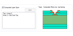
Constraints rules are created for Micro-vias using the Pulsonix Attribute mechanism. This enables designers to easily specify Micro-via sizes and styles to be used from layers which require this specialised technology.
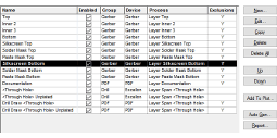
Outputs for via location by layer are available in NC Drill and report format thus ensuring your manufacturing export integrity is maintained right through to the final board production. Drill sets for laser drilling can be output based on layer class and drill type rules.
Fertigungs Ausgaben
Micro-Via Technologie
Passive Bauteile
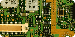
Passive resistors can be printed on inner layers and connected using resistive material. Depending on the manufacturing method, a resist mask or encapsulating coating will be required. Pulsonix handles this by allowing you to associate the necessary additional manufacturing layers for the resistive and other materials with the correct inner copper layer.
Vergrabene Chips
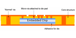
As part of the European funded Hermes project, Pulsonix has been developed well beyond the current commercial capabilities such is the belief that Pulsonix can also be used to help steer new technology into the market. The Hermes project has enabled Pulsonix to introduce the concept of 'thinned' dies and buried semiconductors into inner layer substrates.
Planar Bauteile
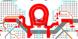
A planar converter may exist on the outer only or through-hole layers and may have a physical body applied to the outer layers. However, part of the footprint consists of copper spirals which are connected by a component via, effectively joining the two footprint pads. By defining the footprint as embedded, the Component can be mirrored in situ and all the inner layers will swap as required. Special DRC properties also allow the checking of correct internal connectivity made on the elements of these components.
Embedded Component Technologie
© 2022-2025 Peschges Variometer GmbH. All Rights Reserved.
Email:
Kontakt |
Produkte |
Service |
Über uns |
